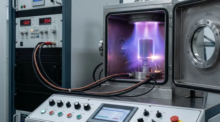
A bias power supply serves as the primary kinetic driver for coating quality during the deposition process. By applying a negative bias voltage—typically between -30 V and -100 V—to the substrate, it accelerates positive ions from the plasma to bombard the tool surface with high energy. This bombardment triggers an atomic mixing effect that is essential for structural integrity.
The bias power supply does not merely deposit material; it actively modifies the coating's microstructure through high-energy ion bombardment. This process is the key to transforming a loose collection of atoms into a dense, highly adherent AlCrSiWN layer with optimized internal stress.
The Mechanism: High-Energy Ion Bombardment
Accelerating Positive Ions
The core function of the bias power supply is to create a controlled electrical potential. By establishing a negative bias on the substrate, it acts as a magnet for positive ions within the plasma cloud.
These ions are accelerated toward the tool surface at high velocities. This kinetic energy is the catalyst for the physical changes in the coating.
The Atomic Mixing Effect
When these accelerated ions impact the surface, they do not just sit on top; they collide with existing atoms. This creates a phenomenon known as atomic mixing.
This intermingling of atoms at the interface is critical. It blurs the distinct line between the substrate and the coating, creating a transitional zone rather than a sharp boundary.
Critical Performance Improvements
Enhancing Subhesion
The atomic mixing effect significantly improves the bond between the AlCrSiWN coating and the cemented carbide substrate.
Without this high-energy bombardment, the coating acts as a distinct layer that can easily peel. The bias creates a mechanical and atomic interlock, ensuring the coating remains fixed under stress.
Maximizing Coating Density
The continuous bombardment during deposition packs the atoms tightly together. This minimizes porosity and voids within the AlCrSiWN structure.
A denser coating translates directly to better wear resistance. It prevents environmental contaminants from penetrating the layer and degrading the tool underneath.
Regulating Residual Stress
Deposition naturally creates stress within a material, which can lead to cracking. The bias power supply plays a vital role in regulating internal residual stress.
By controlling the energy of the arriving ions, the process manages how atoms settle into the lattice. This prevents the buildup of excessive destructive forces inside the coating layer.
Understanding the Operational Window
The Voltage "Sweet Spot"
The benefits of ion bombardment rely on maintaining a specific voltage range, identified in the reference as -30 V to -100 V.
Operating within this window is necessary to achieve the correct level of atomic mixing. If the energy is too low, the ions will lack the momentum required to densify the coating or intermix with the substrate.
Balancing Energy and Structure
The goal is controlled regulation, not aggressive etching. The power supply must provide enough energy to compact the coating and manage stress without disrupting the deposition stability.
Failure to maintain the bias within the optimal range risks producing a coating that is either too porous (low density) or adheres poorly to the cemented carbide substrate.
Making the Right Choice for Your Goal
To maximize the performance of AlCrSiWN coatings, you must view the bias power supply as a tool for microstructural engineering.
- If your primary focus is Adhesion: Ensure the bias is set to trigger sufficient atomic mixing at the start of the process to lock the coating to the cemented carbide.
- If your primary focus is Durability: Maintain the bias within the -30 V to -100 V range throughout deposition to ensure maximum density and minimal porosity.
- If your primary focus is Structural Integrity: Use the bias voltage to actively regulate internal residual stress, preventing premature cracking or delamination.
Ultimately, the bias power supply is the defining factor that separates a superficial surface layer from a robust, industrial-grade protective coating.
Summary Table:
| Feature | Impact of Bias Power Supply | Key Benefit |
|---|---|---|
| Adhesion | Triggers atomic mixing effect at substrate interface | Prevents coating peeling and delamination |
| Microstructure | High-energy ion bombardment packs atoms tightly | Maximizes coating density and minimizes porosity |
| Stress Control | Regulates internal residual stress in the lattice | Prevents cracking and enhances structural integrity |
| Voltage Range | Optimal window of -30 V to -100 V | Ensures balanced energy for stable deposition |
Elevate Your Coating Precision with KINTEK
Unlock the full potential of your AlCrSiWN coatings with high-performance deposition equipment designed for precision. Backed by expert R&D and world-class manufacturing, KINTEK offers a comprehensive range of lab high-temp systems—including Muffle, Tube, Rotary, Vacuum, and CVD systems—all fully customizable to meet your unique thin-film and material science needs.
Whether you are looking to optimize ion bombardment or achieve superior adhesion on cemented carbide substrates, our technical experts are ready to help. Contact KINTEK today to discover how our advanced furnace technology can transform your research and production outcomes.
Visual Guide
References
- Feng Guo. Research on the Performance of AlCrSiWN Tool Coatings for Hardened Steel Cutting. DOI: 10.62051/ijmee.v6n2.01
This article is also based on technical information from Kintek Furnace Knowledge Base .
Related Products
- Multi Heating Zones CVD Tube Furnace Machine for Chemical Vapor Deposition Equipment
- Spark Plasma Sintering SPS Furnace
- Multi Zone Laboratory Quartz Tube Furnace Tubular Furnace
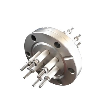
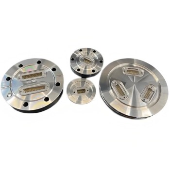
- CF KF Flange Vacuum Electrode Feedthrough Lead Sealing Assembly for Vacuum Systems
- Slide PECVD Tube Furnace with Liquid Gasifier PECVD Machine
People Also Ask
- Why are multi zone tube furnaces particularly useful for nanomaterial research? Unlock Precise Thermal Control for Advanced Synthesis
- What environmental protection applications utilize multi zone tube furnaces? Unlock Precision in Waste Treatment and Green Tech
- What are the advantages of multi-zone tube furnaces? Achieve Superior Thermal Control for Advanced Materials Processing
- What are the benefits of integrating multiple heating zones in a tube furnace? Unlock Precise Thermal Control
- What temperature-related capabilities make multi zone tube furnaces valuable for research? Unlock Precision Thermal Control