The core difference is stark: bulk sintered disc thermistors achieve high densities above 85% of theoretical and exhibit resistivities from 375 to 750 Ω·m, while thick-film thermistors—sandwich, multilayer, or segmented—operate at far lower resistivities of 25–35 Ω·m, a factor of ten to twenty times less. This drop is not a material flaw but a direct consequence of higher porosity in screen-printed films that allows electrode metals to infiltrate the active layer during firing, fundamentally altering the electronic path.
The real story behind the resistivity gap is one of microstructure and processing history. Thick-film geometries sintered at lower temperatures retain intentional porosity. This porosity becomes a pathway for conductor diffusion, slashing effective bulk resistivity while simultaneously unlocking faster thermal response, lower operating voltages, and compact hybrid-integration advantages that dense bulk discs cannot deliver.
The Density–Resistivity Connection
Bulk sintered thermistors and thick-film thermistors share the same spinel oxide chemistry (typically Mn-Co-Fe oxides), but their final density and homogeneity diverge radically.
Why Density Defines Electrical Path
Density dictates how continuous the semiconducting ceramic phase is. High-density bulk discs (>85% of theoretical) present a uniform, low-defect grain network that forces current through the full resistor body, yielding the high 375–750 Ω·m resistivity.
Thick-film layers, in contrast, reach only about 85% of the bulk discs’ density. The residual porosity breaks the ideal continuous path with localized high-resistance voids, but the dominant effect is that this porosity acts as a gateway for electrode metal migration.
The Role of Porosity and Metal Diffusion
Porosity is not just empty space—it becomes a diffusion highway. During film sintering, the printed electrode material (typically PdAg) penetrates into the porous ceramic.
This metallic infiltration effectively shunts portions of the thermistor, halving the apparent resistivity compared to what the dense film would otherwise exhibit. The result is the dramatically lower 25–35 Ω·m range planar geometries show. The porosity that enables faster ion migration thus directly sets the final electrical signature.
Processing Pathways Define the Microstructure
High-temperature lab furnaces orchestrate the density and porosity story through three distinct thermal steps.
Calcination: Building the Spinel Foundation
Raw oxide powders like MnO, CoO, and Fe₂O₃ are first calcined in air at about 900 °C for 2 hours. This solid-state reaction forms the target spinel (Mn₁₋ₓCoₓ)₃O₄. Uniform furnace temperature ensures complete phase conversion and yields submicron particles—essential for repeatable downstream behavior. The density battle starts with the particle packing of this calcined powder.
Bulk Sintering: Maximizing Density
Disc-shaped thermistors are compacted from the calcined powder and sintered at 1200 °C for 30 minutes. This high-temperature drive promotes extensive grain growth and eliminates most porosity, pushing densification well above 85% of theoretical. The outcome: a stable intrinsic resistivity around 750 Ω·m and a B-value near 4200 K. The dense, coarse-grained body is mechanically robust but thermally massive.
Thick-Film Sintering: Preserving Controlled Porosity
Screen-printed pastes on alumina substrates cannot withstand 1200 °C without substrate damage. Sintering instead occurs at roughly 850 °C for only 10 minutes, often with a glass frit additive like Bi₂O₃ to promote binder burnout and adhesion.
The lower temperature and shorter dwell time restrict densification, deliberately maintaining porosity. This porous skeleton then accepts the conductor diffusion that defines the final 25–35 Ω·m planar resistivity. The furnace atmosphere and temperature uniformity remain critical to repeatable R₂₅ values and consistent thermistor constants.
Implications for Thermistor Performance
These structural differences cascade into almost every practical metric beyond the raw resistivity number.
Voltage Scaling and Power Handling
A thick-film thermistor’s low resistivity allows lower applied voltages to achieve the same self-heating or sensing current, simplifying circuit supply design. At the same time, its planar geometry supports higher power dissipation per unit area, spreading heat across the substrate rather than concentrating it in a bulky disc.
Thermal Response Speed
Because thick films are thin and porous, their thermal mass is minuscule. They respond to temperature changes significantly faster than dense discs, making them preferable for transient monitoring and fast-acting protection circuits.
Substrate and Integration Advantages
Planar thick-film designs can be printed directly onto alumina, saving substantial board space in hybrid electronic modules. This integration removes the need for discrete leaded components, trimming assembly complexity and improving reliability in compact designs.
Understanding the Trade-offs
The choice between bulk and thick-film is not universally biased toward one geometry. Each approach solves different engineering problems.
Lower resistivity in thick films is a design enabler, but it also sets a floor on the minimum resistance achievable for a given geometry. If a circuit demands very high base resistance, a thick film may need an impractically long meander, while a simple disc easily hits the target.
The same porosity that accelerates thermal response also introduces sensitivity to environmental contaminants. Humidity or chemical ingress can alter surface conduction paths, potentially requiring a protective overglaze that adds process cost.
Bulk discs, with their dense, coarse-grained structure, deliver superior long-term stability and higher B-values ((\approx)4200 K). This makes them the reference for precision temperature measurement over wide ranges. Thick-film thermistors typically trade a modest reduction in B-value for the thermal and integration perks.
Processing complexity is higher for thick films. Screen printing demands paste rheology control, multiple firing steps, and precise substrate alignment. Bulk discs are simpler to press, sinter, and test, which often translates into lower per-unit costs for discrete sensors.
Making the Right Choice for Your Application
Understand your primary driver, then weigh the material response.
- If your primary focus is high resistance with maximum sensitivity and long-term stability: Lean toward bulk sintered disc thermistors. Their dense microstructure delivers resistivities from 375 to 750 Ω·m and a B-value near 4200 K, ideal for precision temperature sensing where space and response speed are secondary.
- If your primary focus is miniaturization, fast thermal response, and direct substrate integration: Thick-film planar thermistors excel. Their low 25–35 Ω·m resistivity permits low-voltage operation, and their thin porous structure slashes thermal lag, making them the top candidate for hybrid electronic protection and transient monitoring.
- If your primary focus is balancing cost with electrical flexibility: Consider that screen-printed thermistors can be laser-trimmed to target precise resistance values after firing, while bulk discs may need sorting. Evaluate the trade-off between post-process adjustability and the inherent stability of a dense ceramic body.
Ultimately, the same spinel oxide can be a precise, high-resistance sentinel or a lightning‑fast, low‑resistance planar guardian—the furnace profile and geometry you choose write the entire electrical story.
Summary Table:
| Feature / Parameter | Bulk Sintered Thermistors | Thick-Film Thermistors |
|---|---|---|
| Relative Density | High (>85% theoretical) | Lower (~85% of bulk density) |
| Electrical Resistivity | 375 – 750 Ω·m | 25 – 35 Ω·m (10–20x lower) |
| Sintering Parameters | 1200 °C for 30 min | 850 °C for 10 min |
| Microstructure | Dense, continuous grain network | Porous skeleton with electrode diffusion |
| B-Value / Stability | High (~4200 K), superior long-term stability | Modestly lower B-value, fast response |
| Primary Application | High-precision sensing, stable standalone sensors | Planar hybrid circuits, fast transient response |
Precise Sintering Control for Advanced Thermistors with KINTEK
Achieving exact density, controlled porosity, and repeatable resistivity in ceramic thermistors demands strict thermal control. KINTEK provides industry-leading laboratory equipment and high-temperature furnaces—including muffle, tube, vacuum, atmosphere, CVD, and rotary furnaces—all fully customizable to meet your specific research and production requirements.
Whether you are refining high-density bulk ceramics or optimizing screen-printed thick films, our high-precision furnaces deliver the uniform temperature distribution and reliable performance your process requires.
Contact KINTEK today to discuss your furnace requirements with our technical experts!
Related Products
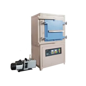
- 1700℃ Controlled Inert Nitrogen Atmosphere Furnace
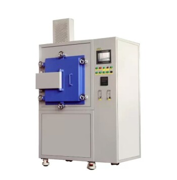
- Controlled Inert Nitrogen Hydrogen Atmosphere Furnace
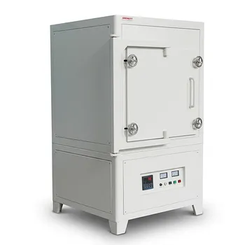
- 1200℃ Controlled Inert Nitrogen Atmosphere Furnace
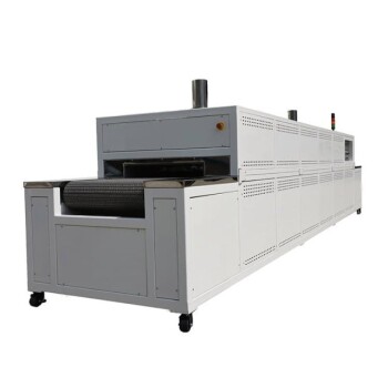
- Mesh Belt Controlled Atmosphere Furnace Inert Nitrogen Atmosphere Furnace
People Also Ask
- How does real-time dilatometric analysis in a controlled-atmosphere furnace optimize PZT ceramic sintering?
- Why is thorough binder burnout necessary before sintering advanced ceramics? Ensure Peak Density & Zero Defects
- How do controlled-atmosphere furnaces support polymer pyrolysis? Master SiC & Si3N4 Ceramic Conversion
- Why is controlled-atmosphere heating required for functional ceramics and sensors? Master Defect Engineering
- How do controlled-atmosphere furnaces verify ceramic powder sinterability? Get True Empirical Densification Data