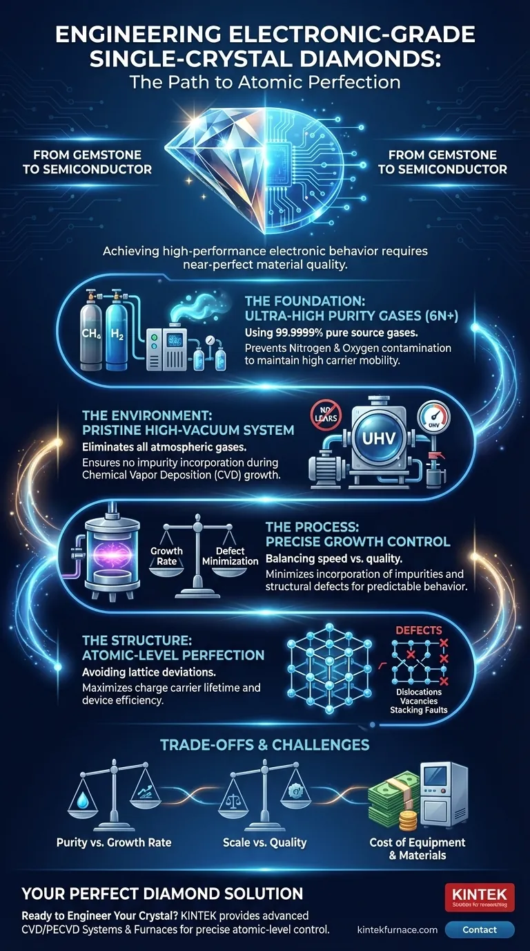
To prepare electronic-grade single-crystal diamonds, you must achieve near-perfect material quality by meeting four fundamental requirements. This involves using ultra-high-purity source gases (methane and hydrogen), maintaining a pristine high-vacuum environment to prevent contamination, and precisely controlling the growth process to minimize the incorporation of impurities like nitrogen and structural defects like dislocations.
The core challenge is not simply growing a diamond, but engineering a flawless semiconductor. While a gemstone’s value lies in its appearance, an electronic-grade diamond’s value is defined by its atomic-level purity and structural perfection, which are essential for predictable and high-performance electronic behavior.
The Foundation: Why Purity is Paramount
The exceptional theoretical properties of diamond—high thermal conductivity, wide bandgap, and high carrier mobility—are only realized in practice when the material is exceptionally pure. Contaminants and unwanted atoms create disruptive flaws in the crystal lattice.
The Role of Impurities
Impurities are foreign atoms that become trapped in the diamond's carbon lattice during growth. Even at concentrations of parts per billion, they can severely degrade electronic performance.
The most critical impurity is nitrogen. It introduces deep energy levels within diamond's bandgap, trapping charge carriers (electrons and holes) and preventing them from moving freely. This effectively kills the material's performance for most semiconductor applications.
Sourcing Ultra-High Purity Gases
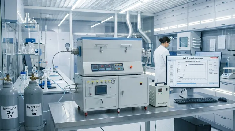
Electronic-grade diamond is typically grown via Chemical Vapor Deposition (CVD). This process uses precursor gases, primarily methane (CH₄) as the carbon source and hydrogen (H₂) an excess.
These gases must be of extraordinary purity, often referred to as "6N" (99.9999%) or better. Any contaminants in the gas supply, such as nitrogen or oxygen, will inevitably be incorporated into the growing diamond crystal.
The Necessity of a Flawless Vacuum System
The CVD growth chamber must be an ultra-high vacuum (UHV) environment. The purpose is to remove all atmospheric gases before introducing the high-purity process gases.
A reliable, leak-free vacuum system is non-negotiable. Even a microscopic leak can introduce a constant stream of atmospheric nitrogen (which makes up ~78% of air), contaminating the diamond and rendering it useless for high-performance electronics.
Achieving Structural Perfection
Beyond chemical purity, the diamond must also have a perfectly ordered atomic structure. Any deviation from the repeating crystal lattice is a defect.
What are Crystal Defects?
Structural defects are interruptions in the perfect pattern of carbon atoms. Common types in CVD diamond include:
- Dislocations: An extra or missing plane of atoms, like a seam or a wrinkle in the crystal fabric.
- Point Vacancies: A single missing carbon atom in the lattice.
- Stacking Faults: An error in the sequence of atomic layers.
The Impact of Defects on Performance
Like impurities, structural defects act as scattering and trapping sites for charge carriers. They disrupt the flow of electrons and holes, reducing carrier mobility—a measure of how quickly charge can move through the material.
High defect densities lead to lower device efficiency, increased electrical resistance, and unpredictable performance, making the material unsuitable for demanding applications like power transistors or radiation detectors.
Understanding the Trade-offs and Challenges
Creating electronic-grade diamond is an exacting process that involves balancing competing factors. Understanding these trade-offs is key to appreciating the difficulty and cost involved.
Purity vs. Growth Rate
There is an inherent tension between the speed of diamond growth and the final quality. Growing a crystal faster often leads to a higher incorporation rate of both impurities and structural defects.
Achieving the highest purity and lowest defect density requires extremely slow, controlled growth conditions, which significantly increases the time and cost of production.
Scale vs. Quality
Maintaining perfect uniformity across a large-area single crystal is a major engineering challenge. It becomes increasingly difficult to ensure consistent temperature, gas flow, and plasma density as the substrate size increases.
This challenge currently limits the size of commercially available, high-quality electronic-grade diamond wafers.
Cost of Equipment and Materials
The required infrastructure is a significant barrier. Ultra-high vacuum components, high-purity gas handling systems, precision power supplies, and in-situ monitoring tools are all exceptionally expensive. The cost of "6N" purity gases is also substantially higher than standard industrial grades.
Making the Right Choice for Your Application
The stringency of these requirements depends directly on your end goal. Not all applications demand the absolute pinnacle of perfection.
- If your primary focus is high-power electronics: Your top priority is maximizing carrier mobility and thermal conductivity. This requires the absolute lowest possible concentration of nitrogen and structural defects.
- If your primary focus is radiation detectors: You need a long charge carrier lifetime and collection distance. The main requirement is minimizing all forms of charge-trapping centers, including both impurities and defects.
- If your primary focus is quantum sensing or computing: You may need an otherwise ultra-pure crystal but with specific, intentionally created point defects (like the Nitrogen-Vacancy center). This requires extreme control over both background purity and the precise placement of the desired defect.
Ultimately, transforming diamond from a passive gemstone into a high-performance electronic material is an exercise in atomic-level control.
Summary Table:
| Requirement | Key Challenge | Impact on Performance |
|---|---|---|
| Ultra-High Purity Gases (6N+) | Preventing nitrogen/oxygen contamination from gas supply | Maintains high carrier mobility and thermal conductivity |
| Pristine High-Vacuum Environment | Eliminating atmospheric leaks (e.g., nitrogen) | Ensures no impurity incorporation during CVD growth |
| Precise Growth Control | Balancing growth rate with defect minimization | Reduces dislocations and vacancies for predictable electronic behavior |
| Structural Perfection | Avoiding lattice defects like stacking faults | Maximizes charge carrier lifetime and device efficiency |
Ready to Engineer Your Perfect Diamond Crystal?
Leveraging exceptional R&D and in-house manufacturing, KINTEK provides diverse laboratories with advanced high-temperature furnace solutions. Our product line, including Muffle, Tube, Rotary Furnaces, Vacuum & Atmosphere Furnaces, and CVD/PECVD Systems, is complemented by our strong deep customization capability to precisely meet unique experimental requirements for electronic-grade diamond growth.
Contact us today to discuss how our tailored solutions can help you achieve the atomic-level purity and structural perfection your research demands.
Visual Guide
Related Products
- Cylindrical Resonator MPCVD Machine System for Lab Diamond Growth
- MPCVD Machine System Reactor Bell-jar Resonator for Lab and Diamond Growth
- 915MHz MPCVD Diamond Machine Microwave Plasma Chemical Vapor Deposition System Reactor
- HFCVD Machine System Equipment for Drawing Die Nano Diamond Coating
People Also Ask
- What are future trends in MPCVD technology? Unlock Next-Gen Materials with AI and Efficiency
- What are the key components of an MPCVD system? Unlock High-Purity Crystal Growth
- How do carbon-containing groups contribute to diamond growth in the MPCVD method? Unlock High-Quality Diamond Synthesis
- What are the essential components of an MPCVD reactor system? Build a Pristine Environment for High-Purity Materials
- What factors influence the quality of diamond deposition in the MPCVD method? Master the Critical Parameters for High-Quality Diamond Growth


