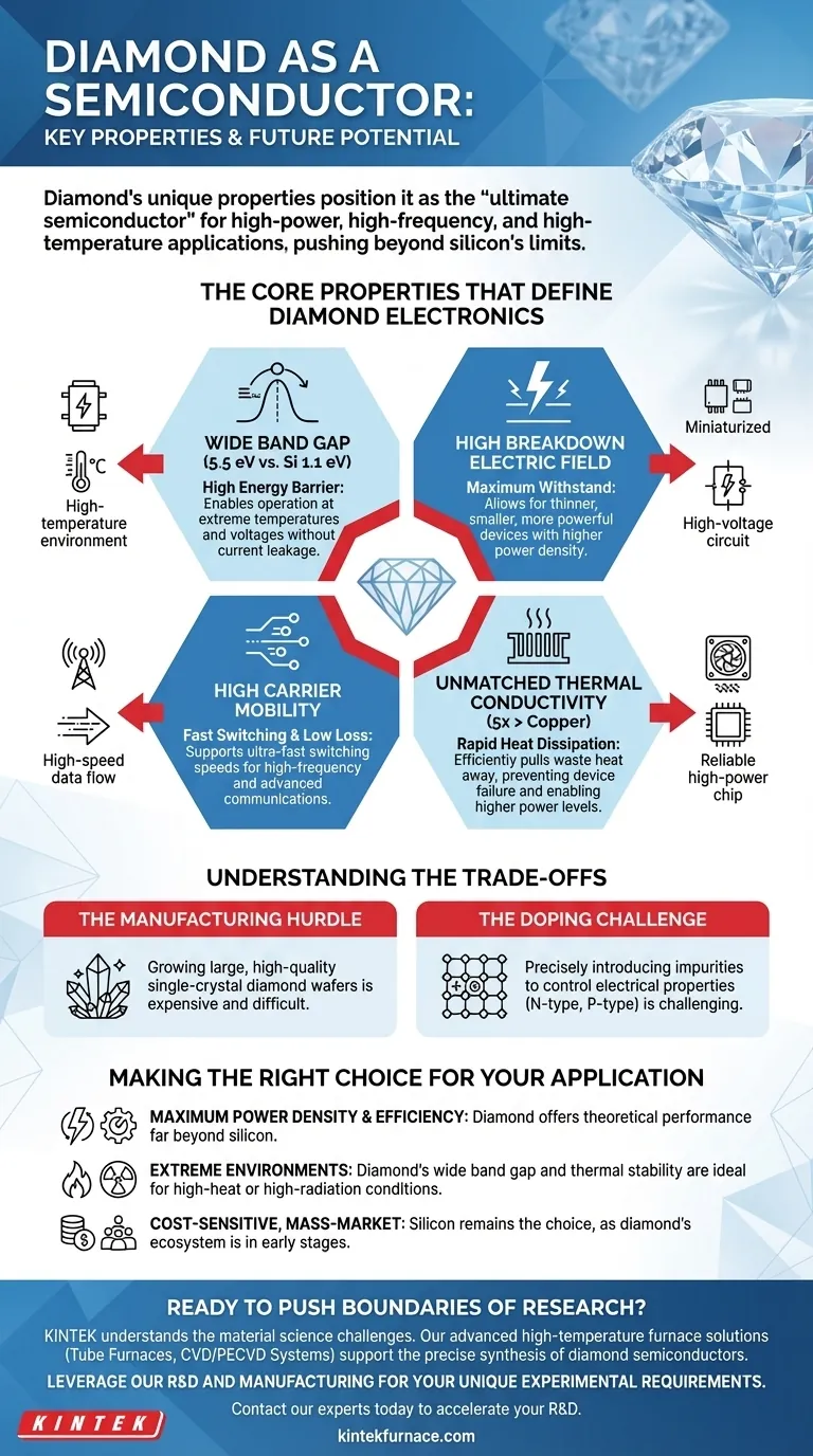
At its core, diamond's promise as a semiconductor stems from a unique combination of four exceptional properties. These are its wide band gap, high breakdown electric field, high carrier mobility, and unmatched thermal conductivity, which together allow it to handle conditions far beyond the limits of traditional materials like silicon.
While silicon built the digital world we know, diamond's properties position it as the "ultimate semiconductor" for the next generation of high-power, high-frequency, and high-temperature electronics. It's not about replacing silicon everywhere, but about enabling performance in the most demanding applications.
The Properties That Define Diamond Electronics
To understand why diamond is so promising, we must look at how each of its key characteristics solves a fundamental limitation in conventional semiconductors.
The Wide Band Gap
The band gap is the energy required to excite an electron and make a material conduct electricity. Diamond's band gap is extremely wide (around 5.5 eV, compared to silicon's 1.1 eV).
This high energy requirement means diamond devices can operate at much higher temperatures and voltages without failing or "leaking" current, which is critical for power electronics.
The High Breakdown Electric Field
Directly related to its wide band gap, diamond has an incredibly high breakdown field. This is the maximum electric field a material can withstand before its insulating properties break down.
A higher breakdown field allows for the creation of devices that are thinner, smaller, and more powerful for a given voltage rating. This leads to higher power density and miniaturization.
High Carrier Mobility
Carrier mobility refers to how quickly charge carriers (electrons and holes) can move through the material when a voltage is applied.
Diamond's high mobility means it can switch on and off very quickly with less electrical resistance. This translates directly to lower energy loss and the ability to operate at much higher frequencies, essential for applications like advanced communications.
Unmatched Thermal Conductivity
This is perhaps diamond's most famous property. It is the most thermally conductive material known to man at room temperature, conducting heat more than five times better than copper.
In an electronic device, waste heat is the enemy of performance and reliability. Diamond's ability to rapidly pull heat away from active regions allows devices to run at much higher power levels without overheating and failing.
Understanding the Trade-offs
While its properties are exceptional, diamond is not a simple drop-in replacement for silicon. The path to widespread adoption faces significant material science and manufacturing challenges.
The Manufacturing Hurdle
Growing large, perfectly uniform, single-crystal diamond wafers is exceptionally difficult and expensive. The cost and complexity of producing high-quality substrates remains the largest barrier to commercializing diamond electronics.
The Doping Challenge
Creating effective semiconductors requires precisely introducing impurities, a process called doping, to control their electrical properties. Doping diamond to create the necessary N-type and P-type materials has historically been far more challenging than with silicon, slowing the development of complex devices.
Making the Right Choice for Your Application
The choice of semiconductor material is always driven by the specific performance goal and economic reality of a project.
- If your primary focus is maximum power density and efficiency: Diamond's combined properties offer theoretical performance for power devices that is orders of magnitude beyond silicon.
- If your primary focus is operation in extreme environments: Diamond's wide band gap and thermal stability make it one of the few viable materials for electronics that must function in high-heat or high-radiation conditions.
- If your primary focus is cost-sensitive, mass-market applications: Silicon remains the undisputed choice today, as the manufacturing ecosystem for diamond is still in its early stages.
Ultimately, diamond represents a frontier in semiconductor technology, promising to unlock new levels of performance where conventional materials simply cannot operate.
Summary Table:
| Property | Why It Matters for Semiconductors |
|---|---|
| Wide Band Gap (5.5 eV) | Enables stable operation at extreme temperatures and voltages with minimal current leakage. |
| High Breakdown Electric Field | Allows for smaller, thinner, and more powerful devices with higher power density. |
| High Carrier Mobility | Supports ultra-fast switching speeds for high-frequency applications and lower energy loss. |
| Exceptional Thermal Conductivity | Efficiently dissipates heat, preventing device failure and enabling higher power operation. |
Ready to push the boundaries of your high-power or high-temperature research?
At KINTEK, we understand the material science challenges of next-generation electronics. Our advanced high-temperature furnace solutions, including Tube Furnaces and CVD/PECVD Systems, are engineered to support the precise synthesis and processing required for cutting-edge materials like diamond semiconductors.
Leveraging exceptional R&D and in-house manufacturing, we provide the thermal processing control and deep customization capabilities essential for your unique experimental requirements. Let us help you achieve the extreme conditions needed to develop the electronics of tomorrow.
Contact our experts today to discuss how our furnace technology can accelerate your R&D.
Visual Guide