To comprehensively assess films produced by Microwave Plasma Chemical Vapor Deposition (MPCVD), a combination of analytical techniques is required. The primary methods used are X-ray Diffraction (XRD) for structural analysis, Raman Spectroscopy for chemical purity, and Scanning Electron Microscopy (SEM) for surface morphology. These tools work together to provide a complete picture of the film's quality.
Assessing MPCVD film quality isn't about a single "pass/fail" test. It's about using a suite of complementary techniques to build a complete profile of the material's structural, chemical, and morphological properties, which are direct outcomes of the deposition process parameters.
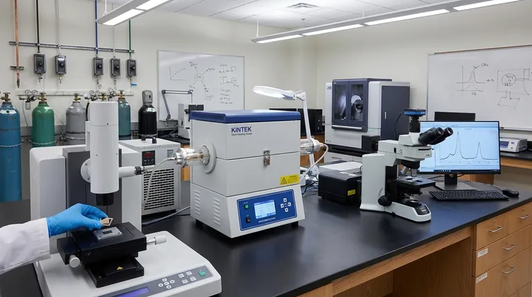
A Multi-Faceted Approach to Film Quality
No single technique can fully define the quality of a thin film. A high-quality film must meet criteria across several domains: its crystal structure, its chemical purity, and its physical surface characteristics. Therefore, a multi-tool approach is the industry standard.
X-ray Diffraction (XRD): Revealing Crystal Structure
XRD is the definitive method for confirming the crystalline nature of the film. It bombards the material with X-rays and measures how they are diffracted by the atomic lattice.
This analysis answers fundamental questions: Does the film possess the desired crystal structure? Is it polycrystalline or single-crystal? XRD data can also be used to estimate grain size and identify preferred crystallographic orientations.
Raman Spectroscopy: Assessing Purity and Stress
Raman spectroscopy acts as a chemical fingerprinting tool. It is exceptionally sensitive to the vibrational modes of molecules, which for carbon materials, allows for a clear distinction between different forms (allotropes).
For diamond films, Raman can precisely quantify the quality by distinguishing the sharp peak of desired sp³-bonded diamond from the broader bands associated with undesirable sp²-bonded graphite or amorphous carbon. It is also highly effective at detecting internal stress within the film.
Scanning Electron Microscopy (SEM): Visualizing Surface Morphology
SEM provides a direct visual inspection of the film's surface at high magnification. It scans the surface with a focused beam of electrons to create a detailed image.
This reveals the film’s morphology, including grain size, grain-boundary structure, surface roughness, and uniformity. It is also the most direct way to identify physical defects like cracks, pinholes, or delamination.
Understanding the Trade-offs and Limitations
While powerful, each technique has inherent limitations. Relying on a single method can lead to an incomplete or misleading assessment of the film's true quality.
What Each Technique Misses
XRD is excellent for ordered crystals but is less effective for quantifying amorphous (non-crystalline) content.
Raman provides superb chemical information but offers no direct insight into the surface topography or large-scale uniformity that SEM provides.
SEM shows the surface morphology in great detail but reveals nothing about the underlying crystal structure or chemical purity of the grains it images.
The Importance of Correlation
The true power of these assessments comes from correlating the results. An SEM image might show a surface with well-formed, faceted grains. Raman spectroscopy confirms whether those grains are high-purity diamond or low-quality graphite. Finally, XRD confirms their crystal orientation and structure.
This combined dataset provides a comprehensive and trustworthy evaluation of the film, allowing you to connect process variables directly to quality outcomes.
Connecting Process to Quality
The quality revealed by these techniques is a direct result of the MPCVD process conditions. Factors like gas mixture, chamber pressure, substrate temperature, and deposition time must be precisely controlled.
These assessment techniques form a critical feedback loop for process optimization. If Raman analysis shows high graphitic content, you know to adjust the gas mixture or temperature. If SEM reveals poor uniformity, you can investigate the plasma distribution or thermal gradients in the chamber.
Making the Right Choice for Your Goal
Use this framework to select the right tool based on the specific property you need to evaluate.
- If your primary focus is chemical purity and bonding quality: Raman spectroscopy is your most critical measurement to distinguish diamond from non-diamond carbon.
- If your primary focus is crystal structure and phase identity: X-ray Diffraction (XRD) is the definitive tool to confirm the crystalline nature of your film.
- If your primary focus is surface uniformity, grain size, and physical defects: Scanning Electron Microscopy (SEM) provides the essential visual evidence.
Mastering this analytical suite transforms MPCVD from a complex art into a controllable, predictable manufacturing science.
Summary Table:
| Technique | Primary Function | Key Information Revealed |
|---|---|---|
| X-ray Diffraction (XRD) | Structural Analysis | Crystal structure, phase identity, grain size, orientation |
| Raman Spectroscopy | Chemical Analysis | Chemical purity (sp³ vs. sp² carbon), stress, bonding quality |
| Scanning Electron Microscopy (SEM) | Morphological Analysis | Surface uniformity, grain size, physical defects, topography |
Need precise, high-quality MPCVD films for your research or production?
Optimizing your MPCVD process to achieve the perfect balance of structure, purity, and morphology requires not just expert analysis but also reliable equipment. At KINTEK, we understand these challenges intimately.
Leveraging exceptional R&D and in-house manufacturing, we provide diverse laboratories with advanced high-temperature furnace solutions. Our product line, including Tube Furnaces, Vacuum & Atmosphere Furnaces, and CVD/PECVD Systems, is complemented by our strong deep customization capability to precisely meet unique experimental requirements.
Let us help you achieve superior results. Contact our experts today to discuss how our tailored solutions can enhance your thin film deposition and quality control processes.
Visual Guide

Related Products
- Multi Heating Zones CVD Tube Furnace Machine for Chemical Vapor Deposition Equipment
- Custom Made Versatile CVD Tube Furnace Chemical Vapor Deposition CVD Equipment Machine
- RF PECVD System Radio Frequency Plasma Enhanced Chemical Vapor Deposition
- Split Chamber CVD Tube Furnace with Vacuum Station CVD Machine
- Inclined Rotary Plasma Enhanced Chemical Deposition PECVD Tube Furnace Machine
People Also Ask
- What future trends are expected in the development of CVD tube furnaces? Discover Smarter, More Versatile Systems
- Why are high-purity quartz boats used for graphene oxide reduction? Ensure Chemical Purity & Thermal Stability
- What functions does glucose perform in lithium-ion sieve synthesis? Enhance Carbothermal Reduction for LiMnO2 Purity
- Why are advanced materials and composites important? Unlock Next-Gen Performance in Aerospace, Auto, and More
- Why is the tube design important in CVD furnaces? Ensure Uniform Deposition for High-Quality Films

